Research
Research
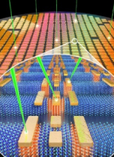
- Nature Electronics (2025) “Quantum-grade transition metal dichalcogenide monolayer semiconductor in wafer scales vicinal van der Waals epitaxy”
- Phys. Rev. Lett. (2024) “Epitaxially defined Luttinger liquid on a MoS2 bicrystal”
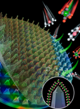
- Nature Nanotech. (2024) “Integrated 1D epitaxial mirror twin boundaries for ultrascaled 2D MoS2 field-effect transistors”
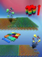
- Nature (2023) “Non-epitaxial single-crystalline 2D material growth by geometrical confinement”
- Nature Nanotech. (2021) “Heteroepitaxial van der Waals semiconductor superlattices”
- Nature Electron. (2021) “Reconfigurable photo-induced doping of two-dimensional van der Waals semiconductors using different photon energy”
- Science Adv. (2019) “Atomically thin three-dimensional van der Waals membrane semiconductors by wafer scale growth”
- Nature Nanotech. (2018) “Generation, transport, and detection of valley-locked spin photocurrent in WSe2-graphene-Bi2Se3 heterostructure”
- Nature Electron. (2018) “Writing monolithic integrated circuits on a two-dimensional semiconductor with a scanning light probe”
- Nature Nanotech. (2017) “Coplanar semiconductor-metal circuitry defined on MoTe2 few-layer polymorphs via heteroepitaxy”
- Nature Nanotech. (2015) “Enhancement of the anisotropic photocurrent in ferroelectric oxides by strain gradients”
- Nature Phys. (2007) “Near-field electrical detection of optical plasmons and single-plasmon sources”
(37673) IBS POSTECH Campus, 79, Jigok-ro, 127beon-gil, Nam-gu, Pohang-si, Gyeongsangbuk-do
- TEL
- +82-54-260-9082~3 (Office)
- VdWQS@ibs.re.kr
Copyright © Center for Van der Waals Quantum Solids at IBS. All Rights Reserved.