Research
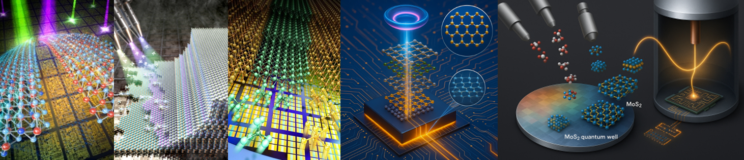
VDW Science
Science “van der Waals materials science”
Epitaxial Molding of vdW Quantum Lattice
Imaging and Spectroscopy Science
Imaging and Spectroscopy Science
- Nature Electronics (2025), “Quantum-grade transition metal dichalcogenide monolayer semiconductor in wafer scales vicinal van der Waals epitaxy”
- Phys. Rev. Lett. (2024), “Epitaxially defined Luttinger liquid on a MoS2 bicrystal”
- Nature Nanotech. (2024), “Integrated 1D epitaxial mirror twin boundaries for ultrascaled 2D MoS2 field-effect transistors”
- Nature (2023), “Non-epitaxial single-crystalline 2D material growth by geometrical confinement”
- Nature Nanotech. (2021), “Heteroepitaxial van der Waals semiconductor superlattices”
- Nano Lett. (2021), “Identification of point defects of atomically thin transition-metal dichalcogenide semiconductors as active dopants”
- Science Adv. (2019), “Atomically thin three-dimensional van der Waals membrane semiconductors by wafer scale growth”
- Nature Nanotech. (2017), “Coplanar semiconductor-metal circuitry defined on MoTe2 few-layer polymorphs via heteroepitaxy”
- Nature Comm. (2015), “Interlayer orientation dependent light absorption and emission in monolayer semiconductor stacks”
- Nano Lett. (2015), “Deterministic two-dimensional polymorphism growth of hexagonal n-type SnS2 and orthorhombic p-Type SnS crystals”,
- Adv. Mater. (2015), “Rotation-misfit-free heteroepitaxial stacking and stitching growth of hexagonal transition-metal dichalcogenide monolayers by nucleation kinetics Controls”
PIs

Moon-Ho Jo
Jong-Hoon Kang

Myungchul Oh
Cheol-Joo KIm

Si-Young Choi
(37673) IBS POSTECH Campus, 79, Jigok-ro, 127beon-gil, Nam-gu, Pohang-si, Gyeongsangbuk-do
- TEL
- +82-54-260-9082 or 9020 (Office)
- VdWQS@ibs.re.kr
Copyright © Center for Van der Waals Quantum Solids at IBS. All Rights Reserved.